Publications
Thickness Scaling Effect on Interfacial Barrier and Electrical Contact to Two-Dimensional MoS2 Layers
S-L Li, K. Komatsu, S. Nakaharai, Y.-F. Lin, M. Yamamoto, X. Duan, and K. Tsukagoshi
ACS Nano 8, 12836–12842 (2014)
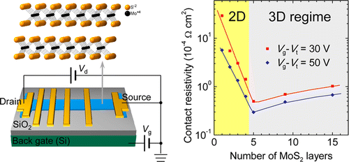
Understanding the interfacial electrical properties between metallic electrodes and low-dimensional semiconductors is essential for both fundamental science and practical applications. Here we report the observation of thickness reduction induced crossover of electrical contact at Au/MoS2 interfaces. For MoS2 thicker than 5 layers, the contact resistivity slightly decreases with reducing MoS2 thickness. By contrast, the contact resistivity sharply increases with reducing MoS2 thickness below 5 layers, mainly governed by the quantum confinement effect. We find that the interfacial potential barrier can be finely tailored from 0.3 to 0.6 eV by merely varying MoS2 thickness. A full evolution diagram of energy level alignment is also drawn to elucidate the thickness scaling effect. The finding of tailoring interfacial properties with channel thickness represents a useful approach controlling the metal/semiconductor interfaces which may result in conceptually innovative functionalities.
UCLA, Department of Chemistry and Biochemistry
607 Charles E. Young Drive East, Box 951569
Los Angeles, CA 90095-1569
E-mail: xduan@chem.ucla.edu
607 Charles E. Young Drive East, Box 951569
Los Angeles, CA 90095-1569
E-mail: xduan@chem.ucla.edu


