Publications
Graphene nanomesh
J. Bai, X. Zhong, S. Jiang, Y. Huang, and X. Duan
Nature Nanotech. 5, 190-194 (2010)
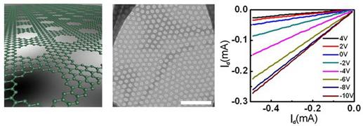
Graphene has significant potential for application in electronics, but cannot be used for effective field-effect transistors operating at room temperature because it is a semimetal with a zero bandgap. Processing graphene sheets into nanoribbons with widths of less than 10 nm can open up a bandgap that is large enough for room-temperature transistor operation, but nanoribbon devices often have low driving currents or transconductances18, 19. Moreover, practical devices and circuits will require the production of dense arrays of ordered nanoribbons, which remains a significant challenge. Here, we report the production of a new graphene nanostructure—which we call a graphene nanomesh—that can open up a bandgap in a large sheet of graphene to create a semiconducting thin film. The nanomeshes are prepared using block copolymer lithography and can have variable periodicities and neck widths as low as 5 nm. Graphene nanomesh field-effect transistors can support currents nearly 100 times greater than individual graphene nanoribbon devices, and the on–off ratio, which is comparable with the values achieved in individual nanoribbon devices, can be tuned by varying the neck width. The block copolymer lithography approach used to make the nanomesh devices is intrinsically scalable and could allow for the rational design and fabrication of graphene-based devices and circuits with standard semiconductor processing.
Authors:
UCLA, Department of Chemistry and Biochemistry
607 Charles E. Young Drive East, Box 951569
Los Angeles, CA 90095-1569
E-mail: xduan@chem.ucla.edu
607 Charles E. Young Drive East, Box 951569
Los Angeles, CA 90095-1569
E-mail: xduan@chem.ucla.edu


