Publications
Graphene-dielectric Integration for graphene transistors
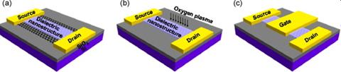
Graphene is emerging as an interesting electronic material for future electronics due to its exceptionally high carrier mobility and single-atomic thickness. Graphene–dielectric integration is of critical importance for the development of graphene transistors and a new generation of graphene based electronics. Deposition of dielectric materials onto graphene is of significant challenge due to the intrinsic material incompatibility between pristine graphene and dielectric oxide materials. Here we review various strategies being researched for graphene–dielectric integration. Physical vapor deposition (PVD) can be used to directly deposit dielectric materials on graphene, but often introduces significant defects into the monolayer of carbon lattice; atomic layer deposition (ALD) process has also been explored to deposit high-κ dielectrics on graphene, which however requires functionalization of graphene surface with reactive groups, inevitably leading to a significant degradation in carrier mobilities. Using naturally oxidized thin aluminum or polymer as buffer layer for dielectric deposition can mitigate the damages to graphene lattice and improve the carrier mobility of the resulted top-gated transistors. Lastly, a physical assembly approach has recently been explored to integrate dielectric nanostructures with graphene without introducing any appreciable defects, and enabled top-gated graphene transistors with the highest carrier mobility reported to date. We will conclude with a brief summary and perspective on future opportunities.
Authors:
UCLA, Department of Chemistry and Biochemistry
607 Charles E. Young Drive East, Box 951569
Los Angeles, CA 90095-1569
E-mail: xduan@chem.ucla.edu
607 Charles E. Young Drive East, Box 951569
Los Angeles, CA 90095-1569
E-mail: xduan@chem.ucla.edu


